Technology
Unlock unparalleled data security and performance with Fully Homomorphic Encryption (FHE) solutions enhanced by silicon photonics. Our advanced hardware keeps your data encrypted at all times while being processed at high speeds, ensuring quantum safety.
FHE Technology
Our technology keeps your data encrypted throughout every stage of processing. Designed for peak performance, it enables complex computations without ever exposing the data, making it ideal for high-impact applications such as blockchain, secure AI, tokenization, federated learning and secure databases.
Standard encryption
Your data is vulnerable
Data decrypted for processing

Fully Homomorphic Encryption
Your data is protected
Data stays encrypted at all times

How it works
We combine the power of optical compute and transport to break through the limitations of conventional computing, unlocking the potential of FHE.
Advantages
Increased sharing of public and private information
Reduced impact of data breaches
Improved cross-border collaboration
Greater privacy for individuals
Enhanced scope for innovation
Secure generative AI
Further information
Enhance your knowledge of FHE, data security, and Privacy-Enhancing Technologies (PETS). Dive into our collection of articles, blogs, and reports.


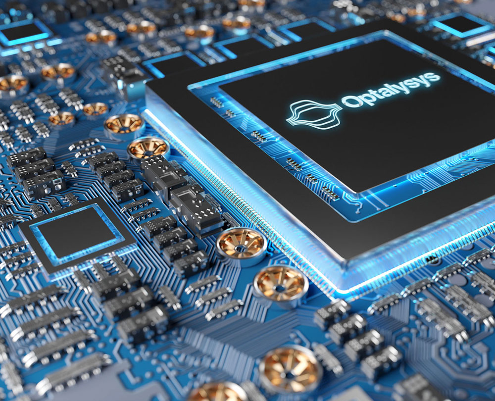
Light-Powered Acceleration
FHE technology is revolutionary, but it’s currently limited by the speed of electrical computing. To overcome these limitations, we’re turning to silicon photonics. This unique technology uses light, rather than electrical signals, to transmit data—much like fiber optics in high-speed internet—but integrated directly into computer chips. By harnessing the power of light, we’re working to accelerate FHE processes to unprecedented speeds. Making FHE a usable, reliable and efficient technology for everyone’s data.


Enhanced
Performance
Integrating FHE technology with silicon photonics significantly boosts overall performance, reduces latency, and enhances encryption speed and effectiveness. Whether you need on-demand, cloud-based, or on-premises solutions, our cutting-edge silicon photonics ensures secure and rapid data processing at unprecedented speeds.
Where electronic computing ends.
We begin.
Our community resource hub
Innovation Lab
Join our unique community hub to develop your FHE skills with expert training, market insights, exclusive content and events.