The MFT System Part 2: Free Space Optics
In part 1 of this article, we explained how we use silicon photonics to control and modulate light with the aim of creating an optical field that contains data we want to process.
The Optalysys approach is very different to the other silicon photonic computing systems which are under development. Like our own designs, these systems use arrays of Mach Zehnder interferometers (MZIs) embedded in silicon to control light and perform multiplications. However, these other optical computing systems are only designed to perform multiplications for the Multiply and Accumulate (MAC) operations that are part of executing many deep learning models. They use many more MZIs to create what is called a “systolic array”, a cascade of processing nodes which perform calculations on information received from nodes further upstream in the data flow. In these models, light never leaves the silicon photonic system.
Optalysys are different; we use silicon photonics to prepare a 2-dimensional field of optical information for nearly instantaneous parallel processing. Light must leave our silicon system so that it can perform a calculation through diffraction. This approach is unique even by the standards of photonic computing, and has some crucial advantages.
Not only can our system be used to efficiently calculate the Fourier transform of an array of data, but it can also be used to perform the same MAC operations that other silicon photonic systems are designed to execute with no additional overhead compared to the systolic array method. We’ll come back to how we can perform general matrix processing tasks using Fourier optics in a later article; for now, we’ll focus on how we make the transition from the silicon photonic stage to the free space processing environment.
Fourier Optics
In explaining how this stage of our system works, it’s helpful to describe some of the basic ideas behind the way in which light travels in free space. Light is a form of electromagnetic radiation, which travels as a wave. Because electric fields and magnetic fields are linked, this takes the form of two waves, representing the electric and magnetic afields, which oscillate at right angles to one another.
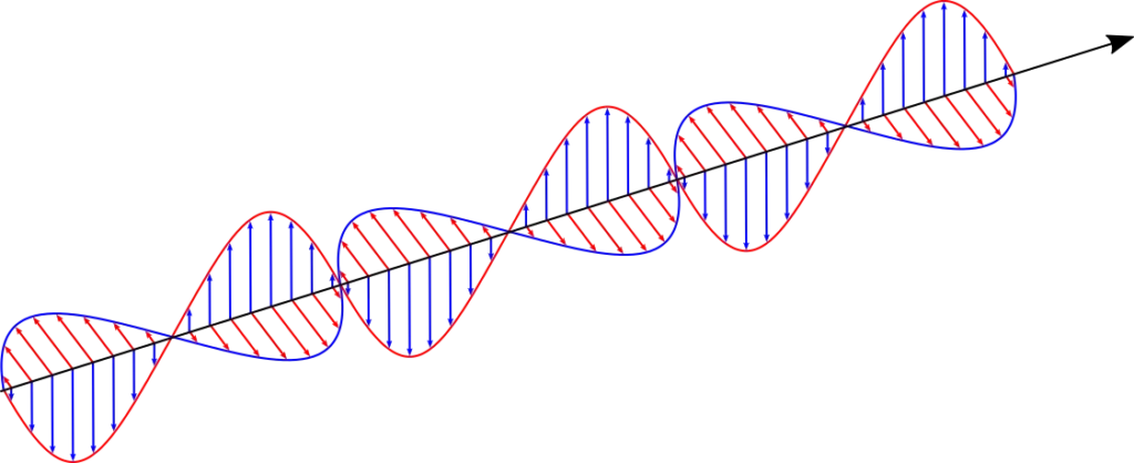
The electrical (red wave) and magnetic (blue wave) fields of a photon oscillate in planes which are at right angles to one another; both are at a right angle to the direction in which the photon is travelling.
For a source of light of constant phase and frequency, the kind emitted by a laser, we can represent the optical field in free space as a continuous wave:
A single wave of a monochromatic optical field, shown for the electric field component only. The lines indicated by the blue arrows represent regions which have consistent phase.
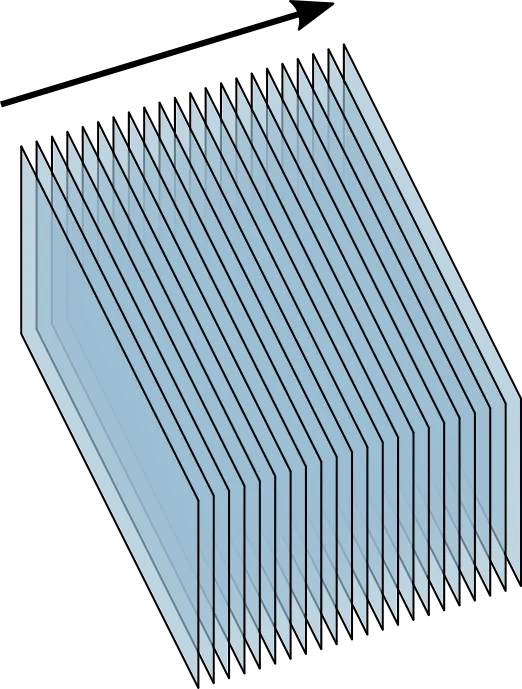
Over a volume of space that contains an optical field, these lines of constant phase collectively describe a series of flat planes.
This is only true when light is travelling in free space, where it can spread out and form a plane wave. In a waveguide or fibre-optic cable, there are boundaries which prevent this spreading.
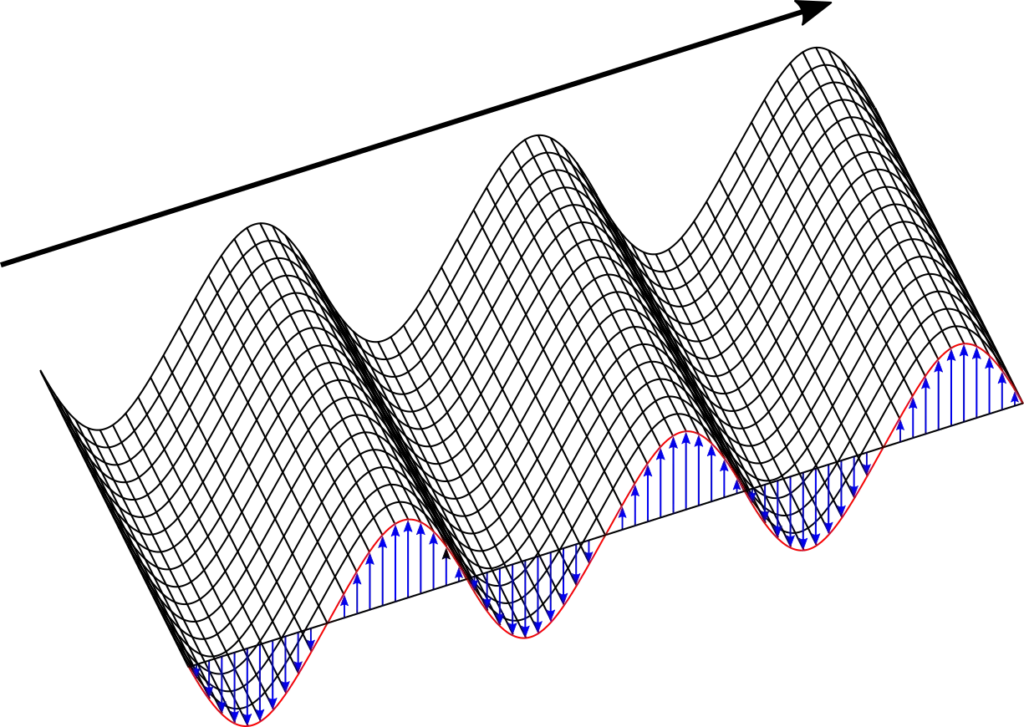
Fourier optics treats the optical field as being a linear superposition of many different plane waves. This is identical to the way in which we can construct a mathematical function by superimposing simple harmonic functions.
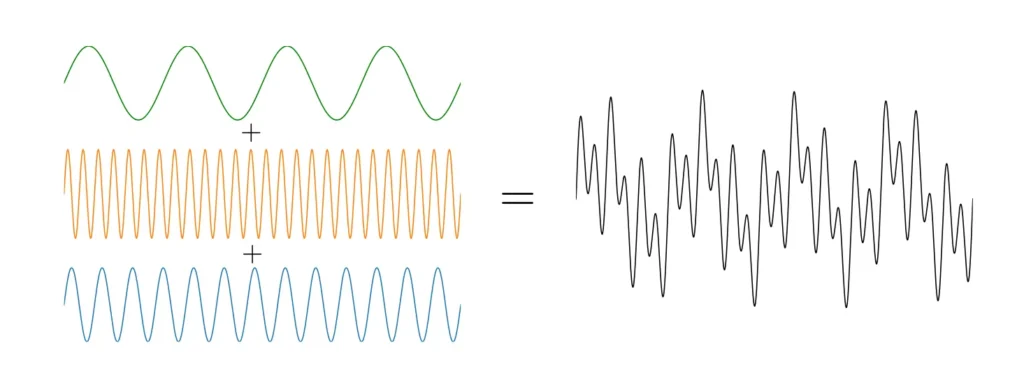
A superposition of harmonic functions to create a new function. The Fourier transform reverses this process, allowing us to isolate the individual contributions from each harmonic.
Crucially this means that the different plane waves can also be separated out. This is the role of a lens in Fourier optics; when a diffracting wavefront made of many different plane waves passes through the lens, the change in refractive index and the curvature of the lens focuses each differing plane wave along a different direction.
By creating an appropriate wavefront, we can use this property to process information in a useful way. To perform this calculation, the light has to travel a distance equivalent to the focal length of the lens. We therefore have to set up an optical input plane, the starting point for the wavefront that arrives at the lens.
Creating the input plane
In our last article, we described how we use a silicon photonic chip to perform the following tasks:
- Split a single source of laser light into many individual beams
- Encode complex values into the phase and amplitude of each beam by using Mach-Zehnder interferometers
- Perform an additional stage of optical multiplication on each beam if required.
We now want to emit that light into free space, creating an optical field which contains a representation of all the data that we want to transform.
Once the silicon photonic system has performed the above steps, the processed light is then carried by waveguides to a 2-dimensional array of grating couplers where it leaves the silicon photonic system. We left a detailed description of how grating couplers work for this article, as the way in which these components work influences the design of the free space section.
Grating couplers
Agrating coupler is a structure cut into a waveguide that uses diffraction to change the direction in which light is travelling. If you were to cut through our silicon photonic chip to show the structure of a grating coupler from the side, it would look something like this:
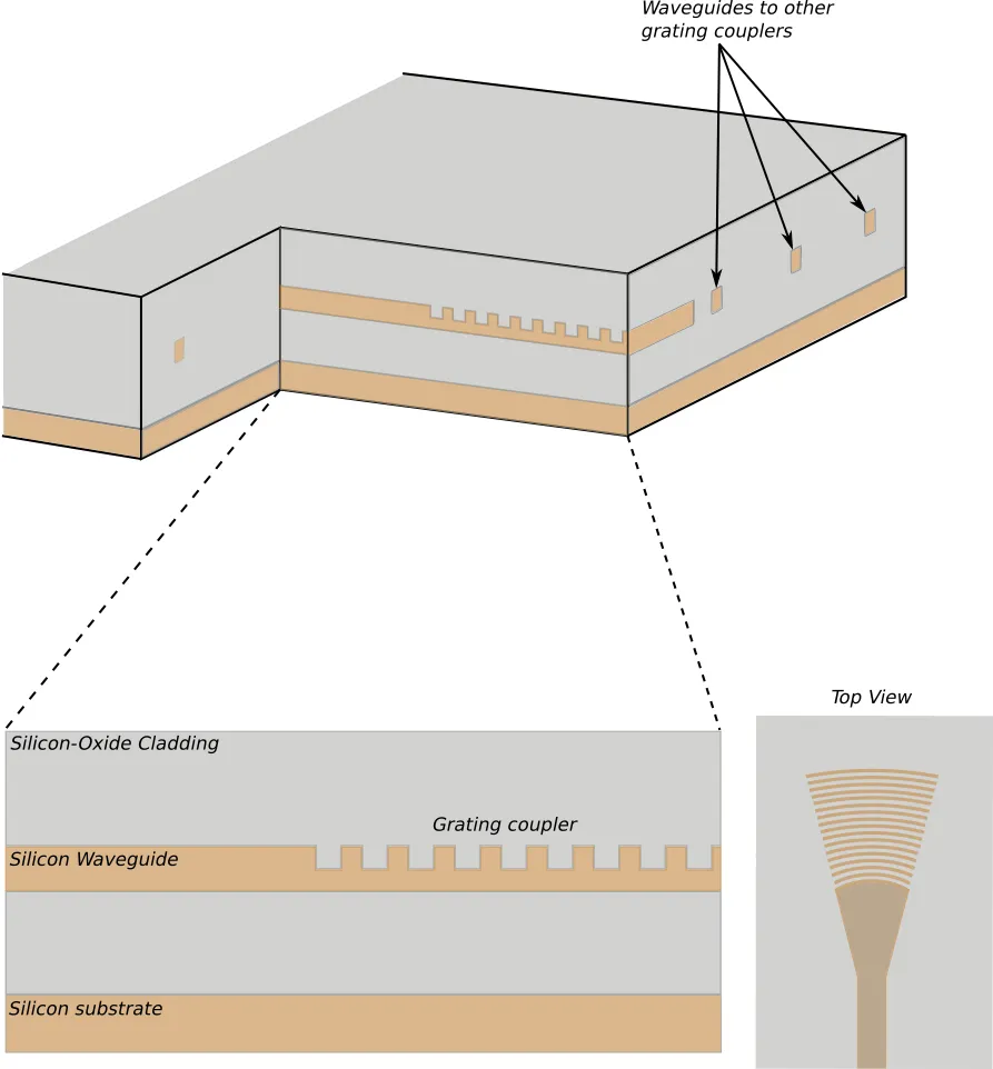
A cutaway diagram of a silicon photonic chip showing the structure of a grating coupler. Light travelling along the waveguide encounters a sequence of flat surfaces that cause it to diffract upwards, out of the chip and into free space. The silicon oxide cladding protects the structure of the silicon photonic components and provides optical isolation.
The structure of the grating coupler is designed to present a series of surfaces to the incoming light that cause it to diffract. In this case the light diffracts upwards, out of the surface of the chip.
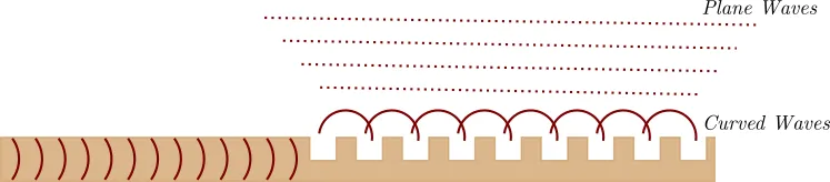
Light travelling down the waveguide encounters the grating coupler and diffracts upwards. The field close to the grating is irregular because the light is emitted as a series of curved wavefronts; further away, these wavefronts overlap and merge to create plane waves.
While normally used to transport or “couple” light between fibre-optic cables and silicon photonics, in our system these grating couplers are used to emit light into free space and capture it at the detection plane. However, the plane of light leaving the grating coupler doesn’t emerge at an exact 90 degree angle, so we need to correct for this. We’ll show how this is done later in this article.
Because each grating coupler is attached to a single waveguide, the 2-dimensional array of grating couplers outputs individual points of light, each of which can be encoded with a different optical phase and amplitude. The number of points of light is a measure of the “resolution” of the system in much the same way that a television or monitor has pixels at a defined resolution (e.g 1920×1080). Our prototype device has a resolution of 5×5, provided by 25 individual grating couplers.
We can perform a Fourier transform using light emitted directly from the grating couplers, but this presents two problems. The first is that the size of the individual grating couplers (relative to the total surface area of the array) is very small. The second is that the light leaving the grating couplers spreads out immediately, weakening the strength of the optical signal and causing additional interference where it isn’t wanted.
To address these problems, we need another component. Enter the micro-lens array.
Micro-Lens array
Amicro-lens array is a flat grid of tiny lenses held in place by a supporting material.
A microlens array, a grid of miniature lenses designed to collect and focus light from tiny optical sources
Developed for other optical applications to capture and focus light onto detectors, we use microlens arrays in our system to
- Capture as much light as possible from the grating couplers and direct (“collimate”) it towards the main lens, reducing the optical loss
- Increase the “fill factor”, the illuminated area of the optical plane.
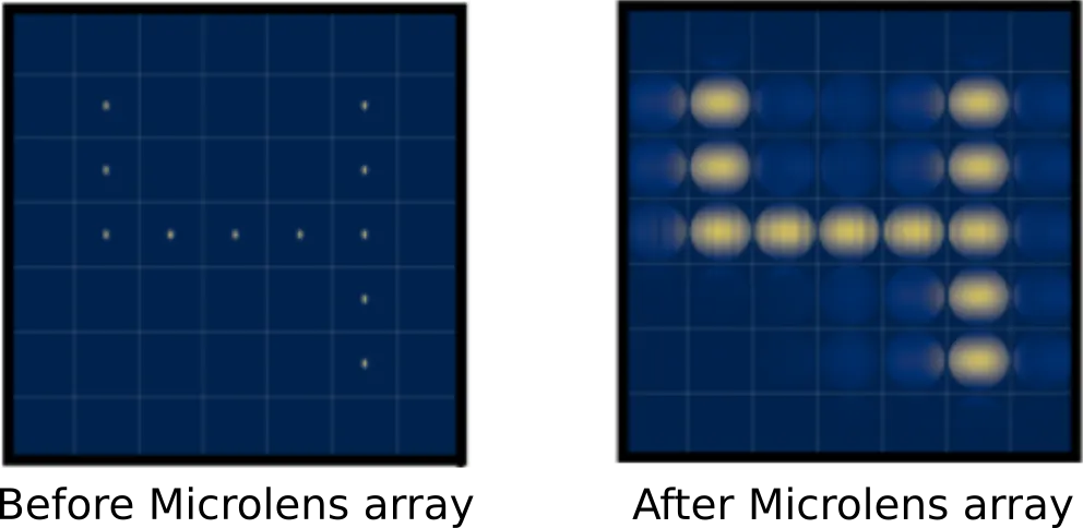
Simulation of the optical plane before and after the microlens array. The left image shows the tiny points of light emitted by the grating couplers. In the right image, the circular microlenses have captured much of the emitted light as it spreads out, directing it towards the main lens.
Once the light from the grating couplers has passed through the microlens array, the optical field is ready for processing. We allow the wavefront to travel through free space, interfering with itself over the length of the free space stage until it strikes the lens.
Prisms
The typical picture of a Fourier-optical system is that of an input plane, a lens, and an output plane arranged in a straight line.
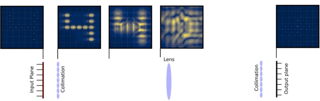
A free-space optical system for performing the Fourier transform, with simulated images of the 2D electric field component of the optical field as it passes through space.
We’ve used this image ourselves when explaining the idea behind our own system, but in reality this presents a problem We’ve used this image ourselves when explaining the idea behind our own system, but in reality this presents a problem when it comes to making the system compact. As the array of grating couplers lies on the surface of the optical chip, this design would mean that the entire free space section would have to point straight up, at a right angle to the surface of the chip! To make matters worse, the detection array would need to be a separate component.
Prisms provide a solution to this problem. Placing a prism over the micro lens array presents a reflective surface to the light that allows it to make another 90 degree turn, such that the beam now travels parallel to the surface of the chip. We can also insert a lens into the middle of the prism, so the free-space optics can be a single block of components.
This lets us use the optics in a much more compact configuration, but it also has an additional useful property; by adjusting the angle of the reflective surface, it allows us to correct the angle of the optical field from the grating couplers.
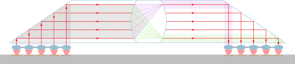
The complete free-space stage, the heart of our optical Fourier transform technology, shown splitting an optical signal into component plane waves. All the components shown here are passive; they consume no power, but are capable of processing information at an almost arbitrary rate.
Now the wavefront is travelling in the correct direction, directed towards the main lens in the system. As it passes through Now the wavefront is travelling in the correct direction, directed towards the main lens in the system. As it passes through the lens, the superimposed plane waves that make up the field are separated and focused along different spatial paths, producing the pattern of bright spots that correspond to the 2-dimensional Fourier transform.
A second microlens array is used to capture as much of this optical field as possible and focus it onto an array of grating couplers which return the light back into silicon photonics.
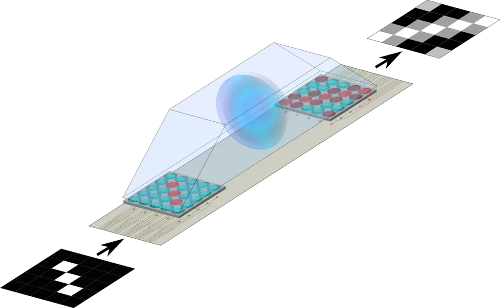
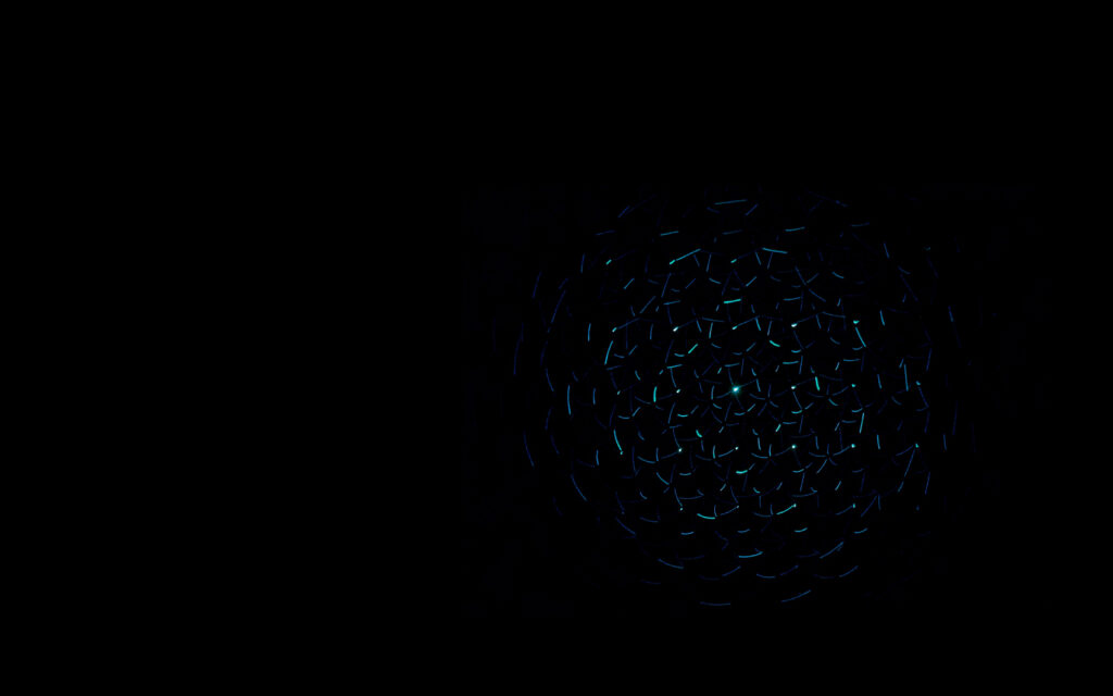
A concept illustration of the system processing data. The input and output images are from real operations performed on the system prototype in our lab.

The optical system as currently set up in the lab. 1: An external laser source is coupled into the optical system. 2: The silicon-photonic chip itself. 3: The prism/lens combination system that performs the Fourier transform and directs the light towards an infra-red camera. There’s no need for the optics to be this big in the final system; we’re just using a larger prism for now while we work on the prototype. 4: The drive electronics that feed digital data into the system.
The calculation is now technically complete, but there is still one final step to perform before we can make use of the information. We have to detect the field, and convert it back into a digital-binary representation. In our next article, we’ll be talking about how we can recover the complex optical signal and send the results back to electronics.