Experiment with FHE acceleration in our new innovation Lab

Introduction

The Multiply and Fourier transform Unit: A Micro-Scale Optical Processor
Written by Joseph Wilson

Table of Contents

The processing of information by means of a coherent optical system has been a proposition for over 50 years. Such systems offer extreme processing speeds for Fourier-transform operations at power levels vastly below those achievable in conventional silicon electronics. Due to constraints such as their physical size and the limitations of optical-electronic interfaces, the use of such systems has so far largely been restricted to niche military and academic interests. Optalysys Ltd has developed a patented chip-scale Fourier-optical system in which the encoding and recovery of digital information is performed in silicon photonics while retaining the powerful free-space optical Fourier transform operation. This allows previously unseen levels of optical processing capabilities to be coupled to host electronics in a form factor suitable for integration into desktop and networking solutions while opening the door for ultra-efficient processing in edge devices. This development comes at a critical time when conventional silicon-based processors are reaching the limits of their capability, heralding the well-publicised end of Moore’s law. In this white paper, we outline the motivations that underpin the optical approach, describe the principles of operation for a micro-scale optical Fourier transform device, present results from our prototype system, and consider some of the possible applications.

Why Optics?

Optical processing is arguably one of the most competitive systems for nonelectronic computation. Fourier optics exploits the property that the electromagnetic optical field projected onto the down-beam focal plane of a standard optical lens contains the 2-dimensional continuous Fourier transform F(x,y) of the field E(x,y) present at the up-beam focal plane.

Figure 1: The 4f optical correlator. A propagating laser beam is modulated by data a, Fourier-transformed by a lens, and then optically multiplied by further modulation with B, which corresponds to the Fourier transform of some original data b. The light then passes through a second lens which performs the inverse Fourier transform and projects the convolution a ~ b onto a plane c, where it is detected by a camera or photodiode array

The canonical example of such a system is shown in Figure 1 in the form of the optical correlator, an optical information processing system dating back to the 1960s which has seen wide use in pattern-matching applications. At the core of optical correlation is the convolution equation, which states that the convolution of two functions is equivalent to the inverse Fourier transform of the element-wise multiplication of the Fourier transform of each function:

The development of artificial intelligence and deep learning has in recent years provided a wealth of novel data processing techniques. Of immediate interest from an optical processing perspective is the Convolutional Neural Network or

CNN. In a CNN, data corresponding to a digital image I(x,y) (or indeed a general 2-dimensional data-set) is convolved with multiple kernel functions Ki(x,y) which extract image features into a series of maps. In machine vision for image categorisation, the combination of these feature maps[1] is then used by a fully connected network to classify the subject(s) of an image. While this is a computationally expensive operation when evaluated directly in the spatial domain (of order O(nm) where n and m are the respective dimensions of I and K), this operation can be expressed as a simple element-wise matrix multiplication (O(max(n,m)) in the Fourier domain by way of Equation 1. Furthermore, both the Fourier transform and the element-wise multiplication may be carried out in parallel by an optical system such that an individual convolution operation can be performed in O(1) time regardless of the image/kernel dimensions, up to the maximum resolution of the system.

However, a Fourier-optical system is not limited to CNN techniques and an ultrafast Fourier transform has many generalised applications in information processing. One of the more pertinent applications, that of novel cryptographic systems, is explored in Section 5.1.

Figure 2: The Optalysys FT:X 2000, a proof-of-concept high-resolution low-speed Fourieroptical computing system

The optical approach offers two primary advantages over conventional electronics:

  • High bandwidth; Optical systems operate by directly modulating an extremely high-frequency carrier; for communications-band 1550 nm light, the associated baseband frequency is nearly 200 THz. An optical system can achieve very high calculation throughput by making use of existing high-speed input devices, modulators and sensors.
  • High connectivity; While propagating through free space, an optical calculation is inherently highly connected and massively parallel. In the potential for all-to-all mapping from a large number of input nodes to a large number of output nodes, this technique is unmatched in conventional integrated microelectronic methods.

This massively parallel calculation in the optical domain is the basis of all Optalysys technology, including our previous FT:X series of Peripheral Component Interconnect Express (PCIE) interfaced optical systems as shown in Figure 2. However, these devices feature large resolutions (> 2 million pixels) and slow operating speeds in the kHz range. This very high resolution and low speed is not suited to CNN applications that require many convolution operations be performed in a short period of time, but use kernels that generally do not exceed 5×5 elements in resolution. The move to a silicon-photonic (SiP) system imposes a practical limit to system resolution (albeit a resolution that exceeds the size of a typical kernel) while offering the potential for operation at multi-GHz speeds in a smaller form factor that better meets the needs of today’s AI applications. The SiP section of our system is shown in Figure 3.

Figure 3: The emissive grating coupler and input waveguides of the Optalysys MFT-SiP prototype, a low-resolution high-speed Fourier-optical computing system.

The micro-scale system developed by Optalysys consists of two basic elements. The first is a SiP multiplication stage for optically encoding and multiplying two complex numbers through the use of two sequential arrays of Mach-Zehnder Interferometers (MZIs). The second is a single 2f Fourier transform stage performed in optical free space. Together, they form the Multiply-and-Fourier Transform (MFT) unit, shown schematically in Figure 4.

Figure 4: A schematic view of our Multiply-and-Fourier Transform optical system, incorporating two MZI stages and a free-space Fourier optics stage. An initial beam of coherent light is split into individual SiP waveguides which each feed two sequential MZIs used to encode data into each beam. These individual beams are then recombined in free space and allowed to diffract before passing through a convex lens, which focuses the beam and projects the Fourier transform of the data onto a detection plane.

[1] Generally after several rounds of pooling and cross-channel summation to reduce the amount of output data

The MFT Unit

3.1 The Multiplication Stage

In the multiplication stage, a beam of 1550 nm infra-red laser light is supplied by an integrated solid state laser. This initial beam is first divided by a branching tree multiplexer and then coupled into waveguides etched in a silicon die. Each waveguide individually feeds two sequential SiP MZIs which are used to alter the phase and amplitude of each beam to encode a complex value. This is shown schematically for a single waveguide and MZI pair in Figure 5.

Figure 5: Schematic diagram of two sequential MZIs fed by a waveguide connected to an optical source. The numbers ϕ1 and ϕ2 are the beam phases accumulated by the field when passing through the upper and lower arms of the first MZI. The phases ψ1 and ψ2 are those accumulated in the upper and lower arms of the second MZI.

Modulation of a beam by an MZI is accomplished by modifying the local speed of light along each arm of the MZI by adjusting the refractive index of the silicon. Assuming a consistent refractive index n along each arm of length l, the associated change in phase is given by Equation 2.

In our prototype device, n is adjusted by altering the local temperature along each arm with an array of micro heaters. The field amplitude after multiplication by the complex value in a given MZI is

                      3.2      The Fourier transform stage

Figure 6: An unmodulated beam of laser light (denoted here by unity) enters the MZI array. The encoding of beam with a complex value into the optical field occurs at MZI 1. This encoded beam then propagates into MZI 2, where it can be multiplied by a second complex value.

The use of two MZI arrays in the multiplication stage is intended to allow the system to emulate the function of a 4f correlator despite the absence of a second free-space stage. In this application model, data corresponding to the FT of an image or other data-set is encoded into the beams by the first MZI stage. The second MZI stage can then be used to perform the element-wise multiplication of these values by the FT of a kernel. The output of the free-space stage acting on the multiplied values will then correspond to the inverse Fourier transform of the Fourier domain multiplication of data and kernel, as shown in Equation 1.

In the above, we assume that the laser input starts as a coherent, monochrome beam containing no encoded data. If the input has already been processed by another optical source, one or more MZIs may not be required, depending on application. The multiplication unit will still act on the input, but both MZI arrays can be set to multiply by 1. This property allows the device to be integrated into a system of other optical components without interfering with previously processed data.

                      3.2         The Fourier transform stage

Following the multiplication stage, light is emitted into free space through a 2dimensional grating coupler (GC) array, and then relayed through a lens onto a second GC array which images the Fourier plane. Since GC arrays typically have a very low fill factor and produce a divergent beam from each “pixel”, a micro-lens

                      3.3       Detection of the optical Fourier transform

array (MLA) is used to create a collimated input plane with a high effective fill factor. Similarly, the second GC plane accepts a convergent beam, and so a second MLA is used to focus the Fourier plane resolution elements down onto the corresponding GCs. The arrangement of grating couplers, micro-lens arrays and the optical field are shown in Figure 7.

Figure 7: Illustrative sketch of a single 2f free-space optical stage. On-chip SiP components are coloured grey, free-space optics are coloured blue, and the zeroth-order optical beam is coloured red. d refers to the spacing between GC elements and f is the focal length. Higher-order diffracted light is shown in fainter red and extends beyond the image to the top and bottom; this light is not transmitted through the system when the MLA is in place.

                      3.3           Detection of the optical Fourier transform

The 2-dimensional Fourier transform performed by an optical system is spatially continuous, in that the electric field E(u,v) at the front surface of MLA2 is defined for all spatial frequencies (u,v) by the electric field E(x,y) at the back (downbeam) surface of MLA1, both of which sit at a focal distance f from the FT lens. The relationship between the spatial frequency and distribution of the electric field is given in Equation 4

                      3.3       Detection of the optical Fourier transform

In a digital system, we want to accurately perform the Discrete Fourier Transform (DFT), which for an input I[m,n] of array dimensions (M,N) can be written as

Since the grating couplers are spatially discrete, the electric field is in reality same-valued over local regions and is not continuous. For an idealised system with pixel pitch d and 100% fill factor, the input electric field is effectively the convolution of a discrete input function with a 2D rectangular aperture of size d. Hence, the output field of an optical Fourier transform contains a finite sum of plane waves given by the the discrete sampling points, which are directly related to the DFT of equation 5

The output field itself represents the squared absolute value of a Fourier transform. The full Fourier transform (including both real and complex parts) can be recovered in a single optical frame through the use of a balanced photodiode array.

There are several factors that affect the precision of the detected Fourier transform. The first is the splitting of the laser power by a branching tree; for an N × N grid of grating couplers, the laser power required to provide each GC with light at a constant intensity scales as N2. The second is that silicon absorbs photons through interactions with charge carriers. The laser power required to provide a stronger signal for detection does not scale linearly, which imposes a practical detection limit of 4 bits.

The use of an optical Fourier transform means that the output is not of the same scale as an integer implementation in electronics. The solution is to consider all optical outputs as relative to themselves; the outputs are then normalised by making the highest value in the output equal to the highest value in the bit range, and applying a linear scaling over the remaining values.

Despite the limitations described above, it is possible to calculate a given optical Fourier transform to an arbitrary degree of precision via bit-shifting. While allowing for higher numerical accuracy, this approach requires the use of multiple FT frames to build the result to the desired accuracy.

Demonstrator device

Optalysys have produced a proof-of-concept prototype system incorporating the above technologies and considerations. This system has a GC resolution of 5 × 5 and the refractive index of the individual MZIs is modulated by thermal means. This limits the practical speed of the system as the use of these modulators introduces thermal cross talk, and heater values must be changed comparatively slowly (on the order of microseconds).

Figure 8: The silicon-photonic prototype, the precursor to a fully bonded unit, as mounted in the demonstrator system. The fibre-optic input for the laser and the coupling optics can be seen on the right. The edge of the prism unit is positioned directly over the emitting GC array.

The prototype system is mounted on a custom-manufactured board of drive electronics that manages received data from a host computer, which is encoded into the system via control of the thermal modulators. 1550 nm C-band laser light is provided by a GoLight tunable light source coupled into a branching tree multiplexer by a fibre-optic connection. The free-space stage of the optics is a combined prism-lens unit which is mounted directly above the grating coupler array. The mounting of the system to the drive electronics, the fibre-optic coupling


and the edge of the prism in position above the emissive grating coupler array can be seen in Figure 8. To facilitate the current calibrations being performed on the device, no MLA is present at either the emissive or receiving plane, thus higher order light is transmitted alongside the dominant Fourier plane elements. The effects of this additional light are visible in the results presented in the following Section.

4.1       Results

The following results show the input pattern to the device, the anticipated intensity readout as calculated digitally, and the directly observed output plane. These results are provisional for a device currently undergoing calibration and characterisation. To make the calibration easier, we restricted ourselves to three possible values for each input pixel: −1, 0, or +1. We are currently in the process of performing a finer calibration which will allow for a broad range of real and complex values. Pixel positions are indicated by the label on the axes.

For Figures 9-13, we provide a root mean squared (RMS) error as calculated through the following method. We first normalize the output image so that its values lie between 0 and 1. We then compute the square of the difference with the squared absolute value of the Fourier transform of the input image, average the result over the 25 pixels, and take the square root. This result provides an estimate of the error on each pixel. As can be seen below, this error is smaller than 0.20, and smaller than 0.15 for most of the figures. We expect that a more precise calibration will bring the errors down to less than 0.1 and allow the output to be measured with at least 2 bits of accuracy.

Figure 9: A black (inverse) diagonal. Input values are −1 (black), 0 (grey), and 1 (white). The total RMS error is 0.14.

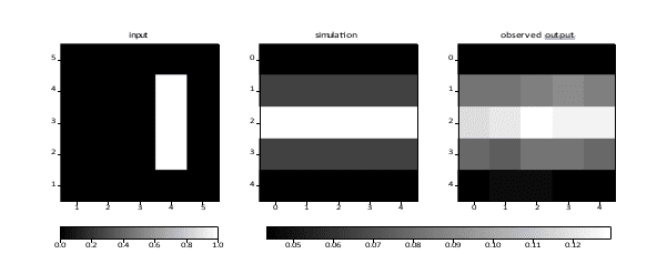
Figure 10: A small offset bar. Input values are 0 (black) and 1 (white). The total RMS error is 0.12.

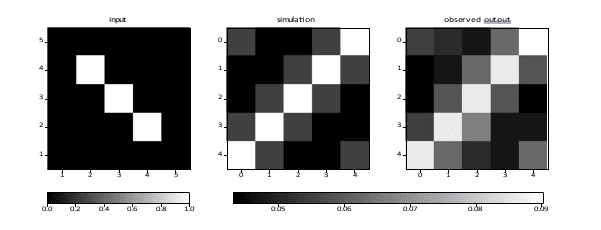
Figure 11: A diagonal pattern. Input values are 0 (black) and 1 (white). The total RMS error is 0.17.

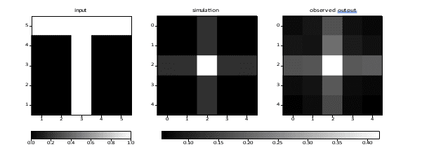
Figure 12: A T-shape. Input values are 0 (black) and 1 (white). The total RMS error is 0.13.

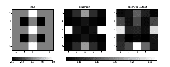
Figure 13: A set of vertical and horizontal line patterns. Input values are −1 (black), 0 (gray), and 1 (white). The total RMS error is 0.14.

The optical device can also be used to compute the full complex Fourier transform of an input by comparing the measured intensities of the output with that of a reference. In the future, this comparison will be performed using balanced photodiodes, allowing to measure both the amplitude and phase in one frame. As a preliminary step, we developed a method to compute the complex Fourier transform from images of the output plane for different outputs.

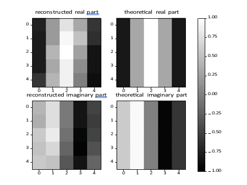
Figure 14: Fourier transform for an input with one bright pixel at position (2,1).

Figures 14 and 15 show results for the Fourier transform for two inputs having


4.2      Route to the future

one pixel in its “on” state each. In each figure, the left panels show the real and imaginary parts of the Fourier transform as obtained using the optical device, and the right panels show the exact discrete Fourier transform of the input. A precise estimate on the complex Fourier transform will require a more precise calibration, which is in progress. However, as illustrated on these two images, preliminary results indicate good accuracy. (At the moment, the RMS error is close to 20%.)

As for the squared absolute value, we expect to reach at least two bits of accuracy.

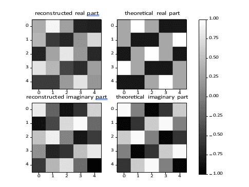
Figure 15: Fourier transform for an input with one bright pixel at position (2,3).

4.2.1          PN Junction Mach Zehnder Interferometers

By far the most significant increase in system operating speeds is offered by adopting an alternative modulation method to the thermal modulators currently used on the demonstrator device. SiP MZIs are also available in the form of the PN-junction MZI, which manipulates the charge carrier density in doped silicon via broadening of the junction depletion layer to dynamically alter the refractive index. Such MZI arrays can be driven at very high speed (up to 50 Gbits/s per MZI) with 4-level Pulse Amplitude Modulation (PAM4).

4.2.2        Systems Integration

The extreme operating speed and throughput of an optical system requires additional consideration as to the manner in which it is integrated into an electronic host. An example is an optical device operating at 9 × 9 resolution at 10 GHz with a detection depth of 2 bits, which has a maximum throughput for FT calculation of 1.62 TBits/s. Higher operating speeds, resolutions and bit-depth are entirely plausible with current technology. Depending on these factors and the device-level integration of the optical system, this throughput may exceed the rate at which data may be transferred over conventional electronic interconnect standards. If used as a desktop co-processor through the same Peripheral Component Interconnect Express (PCI-e) framework as a Graphics Processor Unit (GPU), such a device would effectively reach the Von Neumann bottleneck even for next-generation data transfer standards such as PCI-e v6.0, which supports 128 GB/s (1.024 TBits/s) per direction with a 16-lane configuration. As a component in a stand-alone unit such as a PC motherboard or server rack, achieving peak performance for an MFT unit will likely require the development of a dedicated high-throughput connection positioned near to key processing units and memory.

To take full advantage of the high-speed operation capabilities of the MFT unit in the near future, we therefore suggest integration into existing optical applications. The native use of 1550 nm light in both the MFT unit and the high-bandwidth optical transceivers currently used in data-centres makes the embedding of the MFT unit in these inherently optical systems a natural proposition. The versatility of the Fourier transform and the very high data throughput the device can manage provides significant scope for the transformation of data in-flight. This would allow a range of applications to work at speeds that vastly exceed their current digital implementation. In this use-model, we envisage a world in which data transmitted to the cloud for processing in a neural network arrives on the server having already been converted into a more efficient representation in the Fourier domain as it passes through the network connection, without incurring the time and energy intensive use of the digital Fast Fourier Transform. Alternatively, as the need for quantum-secure communications in the near future becomes more pressing, an MFT unit embedded into an optical transceiver could support the rapid execution of operations that support next-generation lattice-based cryptography. We provide more detail on this application in the following Section.

Applications

The 2-dimensional Fourier transform lies at the core of the Optalysys device. While designed to support additional AI-specific operations, the potential of the system as a means of performing an ultra-fast discrete Fourier transform is marked. While many applications benefit from faster computation of the Fourier transform, we consider the subject of cryptography a prime example due to the time-critical nature of encrypting and decrypting information in a modern communications infrastructure.

5.1      Cryptography

Cryptography secures the digital world around us by obscuring the information contained in data to all but the legitimate parties who are given access to it. The fundamental concept that lies behind all cryptography is the notion that there are certain mathematical functions which are easy to perform but very hard to reverse. In many current cryptographic systems that secure the exchange of data between two digital systems (such as public-key cryptography), the “easy” step is multiplying together two large prime numbers, while the “hard” step is finding both of the primes which were multiplied together to return a very large number. While these systems are secure at the moment, technological advances in quantum computing pose a threat to this paradigm. For example, Schorr’s algorithm is a technique that can only be executed on a quantum computer, but offers a way of finding large prime factors in a time-scale that makes attacking prime-based cryptography plausible.

Awareness of this potential threat has in recent years spurred a sustained search for cryptographic techniques that do not share this vulnerability. While a number of alternatives have been proposed, one of the most promising is Lattice-based cryptography (LBC). The security of LBC is not based on the difficulty of factoring large primes but on the difficulty of solving problems on lattices, specifically what is known as the “shortest vector” problem. In mathematics, a lattice refers to a grid of discrete points where the entire grid can be constructed using simple instructions applied to a given set of vectors known as a basis. Crucially, any lattice can be constructed using many different basis sets; the shortest vector problem requires an attacker to find the shortest vector in the lattice given a basis of much larger vectors. While conceptually simple, the shortest vector problem is categorised as NP-hard, meaning that there is no known algorithm for its solution in either classical or quantum computing.

Besides demonstrating mathematical security, a useful cryptographic system for the digital age must also be able to encrypt and decrypt data at very high speed. LBC is heavily reliant upon the Fourier transform, which is used to efficiently perform point-wise polynomial operations on the lattice, and thus makes extensive use of computational techniques such as the Cooley-Tukey Fast-Fourier Transform (FFT). Indeed, much effort [1,2] has been made on the behalf of LBC to implement more efficient FFT techniques for both the underlying arithmetic and the practical implementation on hardware in an attempt to overcome the O(nlog n) scaling of the Cooley-Tukey scheme. Given the inherent O(1) calculation time of a single discrete Fourier transform in an optical system and the very high speeds a siliconphotonic system may achieve, our device has the capacity to vastly accelerate the practical implementation of lattice-based methods such as the SWIFFT hashing function or NTRU key exchange.

A very recent development of further interest is lattice methods for performing what

5.2      Deep Learning

is known as Fully Homomorphic Encryption, or FHE. An FHE scheme can encrypt data in such a way that the underlying relationships in a data-set are preserved, allowing addition and multiplication operations to be performed even on encrypted data. This has long been considered a significant goal in cloud computing as FHE allows for sensitive data (such as financial or medical information) to be encrypted, sent to the cloud for analysis by a machine learning network, and then returned to the originator without ever leaving a strongly encrypted state. IBM has released an FHE developer toolkit that includes a demonstration of a machine learning network performing inference on an encrypted data-set to demonstrate that this practical aspect of FHE is no longer hypothetical. From both a security and legal perspective, FHE bypasses many of the issues that prevent cloud computing from reaching its full potential, and is set to revolutionise the field.

However, while mathematical operations can be performed on FHE-encrypted data, it is also known to be exceptionally slow and computationally demanding to do so. As with other lattice methods, FHE makes extensive use of the FFT function to the degree that at least one FHE method (Fully Homomorphic Encryption over the Torus, or TFHE) requires a dedicated Fourier processor [2] to run on a practical time-scale. Our system therefore offers the possibility for the dramatic yet efficient acceleration of this groundbreaking technology with the corresponding benefits to both industry and society at large.

Deep learning commonly makes use of high-level frameworks to streamline the construction of network architectures and efficiently execute computations. Our system is designed for integration into common deep learning languages and systemisations such as TensorFlow, Keras and PyTorch via API calls. The prototype device currently supports the input of array data (Python numpy format) into the system via a single Python import: SiliconPhotonicsDevice and optical Fourier transform function: oft(), with all management of the encoding and optical systems handled by the supporting electronics for the device.

5.2.1            Projected performance in the AlphaFold Protein-prediction CNN

To provide an estimate of the speed of the optical system in deep learning tasks, we consider the protein structure prediction tool AlphaFold [3,4]. Developed by Alphabet’s Deepmind group and best-in-class at the 13th Critical Assessment of protein Structure Prediction (CASP 13), AlphaFold uses an extremely deep ResNet Artificial Neural Network architecture to predict the folded structure of proteins. The network is trained on a massive data-set of other proteins sourced from the Protein Data Bank (PDB) and learns features from the the 1-dimensional chain that correspond to the folded 3-dimensional structure. In creating the input data for the prediction of a given protein structure, AlphaFold assembles a 128 channel block of 2-dimensional inputs by applying a range of existing bio-structural data analysis techniques to the 1-dimensional amino-acid sequence of the given

5.2      Deep Learning

protein.

To predict the contact map or “distogram” (the 2-dimensional map that describes the 3-dimensional distances between individual elements of the protein chain), AlphaFold applies 4 slightly different network configurations or “replicas” to the data. To reduce memory usage, each input channel is repeatedly divided into non-overlapping 64×64 crops. An inference pass on a 2-dimensional 64×64 crop of a single channel is performed by a ResNet architecture that consists of 220 individual residual blocks in which the crop is repeatedly convolved with a 3×3 kernel with varying pixel dilation (alongside an Exponential Linear Unit (ELU) activation function and Batch Normalisation per block) and sees the performance of approximately 13,629,440 individual 3×3 convolution operations.

The convolution operations are performed on single-precision 32-bit floats. Using the equivalent of 8 cores (with hyperthreading) on an Intel i7-8700k operating at 3.7 GHz which consumes 86.2 watts of power when under full load, a single pass of a 64×64 crop through the ResNet architecture is performed in an average of 0.71 seconds as determined by inserting time reports into the relevant sections of the CASP-13 version of the AlphaFold source code. It is assumed that the convolutions, as the most computationally expensive operations, account for the bulk of the computational time.

An initial conservative estimate for an optical system is that of a unit with 5×5 resolution operating at 500 MHz with 4-bit precision and consuming 20 watts of power for the optical components. Of course, additional power is required for the surrounding drive electronics that manage the loading, saving and transfer of data; these are specific to the implementation of the device in a system, and so no estimate of their power consumption is given here. It is assumed that the Fourier transform of the pre-trained filters is already known and that no calculation overhead is required for this process at runtime. As both real and imaginary components are recovered simultaneously in an optical system, 8 frames in total (including both forward and inverse Fourier Transforms) are required to match the equivalent accuracy of two 32-bit NVIDIA CUFFT Fourier Transform operations, in which the real and imaginary components are separately represented by 16 bit values. Only 4,759,040 5×5 convolutions are required to match the equivalent number of 3×3 convolutions[1]. Under these values, the total processing time for the network acting on a 64×64 crop is 0.076s.

This would represent an improvement in power efficiency by a factor of 40, and an improvement in processing speed by a factor of 9.32, in comparison to an Intel i7-8700k applied to the same task.

While AlphaFold uses 32 bit floats, recent research [5, 6] has demonstrated that deep learning networks for tasks such as image classification and speech recognition can be trained on 16-bit hardware and can successfully perform inference using inputs of just 2-4 bits. Under such a low-precision paradigm, the form factor and power efficiency of our device makes it a natural contender for performing extremely high-speed image recognition in mobile applications such as hand-held electronics, edge IoT devices, and self-driving automotive solutions.

[1] Convolution with a 3×3 kernel may be performed for higher input data resolution by using a higher-resolution Fourier transform of the 3×3 kernel

Conclusion

Optalysys have developed a novel micro-scale optical processor for optically performing calculations based upon 2-dimensional Fourier transform operations. We have demonstrated how the combination of silicon-photonics and classical freespace optics can provide unique and potent benefits for performing calculations at the very physical limits of speed and efficiency. The vast gains in performance made possible by this technology will not only accelerate existing applications, but spur the development of new approaches and methodologies for data processing that can best utilise the staggering gains in computational power that have been unlocked by our work.

References

  • Thomas Pöppelmann and Tim Güneysu. Towards efficient arithmetic for lattice-based cryptography on reconfigurable hardware. In Lecture Notes in Computer Science (including subseries Lecture Notes in Artificial Intelligence and Lecture Notes in Bioinformatics), 2012.
  • Ilaria Chillotti, Nicolas Gama, Mariya Georgieva, and Malika Izabachène. TFHE: Fast Fully Homomorphic Encryption Over the Torus. Journal of Cryptology, 2020.
  • Andrew W. Senior, Richard Evans, John Jumper, James Kirkpatrick, Laurent Sifre, Tim Green, Chongli Qin, Augustin Žídek, Alexander W.R. Nelson, Alex

Bridgland, Hugo Penedones, Stig Petersen, Karen Simonyan, Steve Crossan,

Pushmeet Kohli, David T. Jones, David Silver, Koray Kavukcuoglu, and Demis Hassabis. Protein structure prediction using multiple deep neural networks in the 13th Critical Assessment of Protein Structure Prediction (CASP13). Proteins: Structure, Function and Bioinformatics, 2019.

  • Andrew W. Senior, Richard Evans, John Jumper, James Kirkpatrick, Laurent Sifre, Tim Green, Chongli Qin, Augustin Žídek, Alexander W.R. Nelson, Alex

Bridgland, Hugo Penedones, Stig Petersen, Karen Simonyan, Steve Crossan,

Pushmeet Kohli, David T. Jones, David Silver, Koray Kavukcuoglu, and Demis Hassabis. Improved protein structure prediction using potentials from deep learning. Nature, 577(7792):706–710, 2020.

  • Suyog Gupta, Ankur Agrawal, Kailash Gopalakrishnan, and Pritish Narayanan. Deep learning with limited numerical precision. In 32nd International Conference on Machine Learning, ICML 2015, 2015.
  • Naigang Wang, Jungwook Choi, Daniel Brand, Chia Yu Chen, and Kailash Gopalakrishnan. Training deep neural networks with 8-bit floating point numbers. In Advances in Neural Information Processing Systems, volume 2018December, pages 7675–7684, 2018.

Subscribe

Sign up with your email address to receive news and updates from Optalysys.

Please enable JavaScript in your browser to complete this form.
We respect your privacy.