
Silicon photonics: our approach to acceleration
Fully Homomorphic Encryption at the speed of light
The rise of silicon photonics
For decades, the world of computing has relied on electronic circuits to process information. But as demand for faster, more efficient computing grows, we’ve hit a wall; power consumption is skyrocketing, and traditional processors struggle to keep up.
Enter silicon photonics—a revolutionary field that uses light instead of electricity to transmit and process information.
Silicon photonics emerged in the late 20th century as researchers sought ways to improve data transmission in telecommunications. Optical fibres had already transformed long-distance communication, but the challenge was integrating this technology into microchips.
By the early 2000s, breakthroughs in fabrication techniques enabled light-based components to be built directly onto silicon chips, leading to rapid adoption in data centres, high-speed internet, and advanced sensing technologies.
Today, silicon photonics is a cornerstone of modern computing infrastructure. But at Optalysys, we’re taking it a step further—using light to perform computations, not just transmit data.
Why light? The power of optical computing
Traditional electronic processors face two major bottlenecks:
- Speed limits – electrons moving through wires create heat and resistance, limiting how fast processors can run
- High energy consumption – As computation increases, so does the power (and spend) required, making large-scale processing unsustainable
Light, on the other hand, offers a game-changing alternative:
- Faster processing – light waves move at incredible speeds and can process information in parallel
- Energy efficiency – optical computing requires significantly less power than electronic circuits
These advantages make silicon photonics the perfect foundation for next-generation computing solutions—including Fully Homomorphic Encryption (FHE).
Accelerating privacy with the power of light
At Optalysys, we’ve developed a silicon photonics-based approach to computing that is specifically designed to accelerate FHE operations.
This diagram illustrates the core principles of our approach:
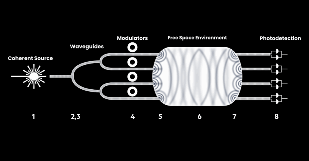
- Laser light is injected into the system
- This light travels through a channel (called a “waveguide”) cut into the silicon
- The waveguide splits into multiple sub-channels, each carrying a portion of the original laser beam
- Modulators adjust the optical properties of each sub-beam, encoding information into the light
- All sub-beams are emitted into a free-space environment within the silicon chip
- As the beams travel, they interfere with each other, performing complex mathematical operations
- This interference naturally executes the core processing workload required for FHE computations
- The final output is detected and converted back into digital information
The future is fast
LightLocker™ Node makes FHE practical for the blockchain ecosystem today. But to power a global, encrypted internet and handle the immense workloads of future secure AI and Web3 applications at global-scale, we must push beyond the limits of electronics.
The ultimate bottleneck becomes the energy and time it takes to move electrons. That is why our technology roadmap leads to silicon photonics – computing with light.
By using photons instead of electrons, our future optical accelerators will unlock further orders-of-magnitude gains in speed and power efficiency. This isn’t just about faster FHE; it’s about building a fundamentally new class of compute infrastructure, capable of powering a truly secure and private global web.
Want more like this delivered straight to your inbox?
Subscribe to stay in the loop