The MFT System Part 1: Silicon Photonics
In our first article, we talked about the basic ideas behind our optical Fourier Transform chip and why we made it a reality. In the next few articles, we’ll be going into greater depth on our system and how it works. We begin here by describing how we can take digital data and encode it into an optical field that can be processed at the speed of light.
Our technology is designed to perform a mathematical function called a 2-dimensional Fourier transform at very high speed. In our system, this calculation is performed through a combination of optical interference and the properties of simple convex lenses. The physical result of that calculation is a 2D pattern of light of varying intensity and phase. To make the system useful, we need to be able to:
- Convert information from a digital representation into an optical field
- Allow that field to interfere with itself and pass through a lens, a process which separates out light of different phases
- Detect the result, and then convert that signal back into a digital representation.
This method sounds like a lot of extra work, but there are some significant advantages to it that make it worth the effort.
The first is that our optical calculations are performed in parallel through interference, so performing a calculation on more data by adding more optical components doesn’t increase the runtime. In fact, adding more data increases the effective performance of our system, as we carry out the equivalent of n log(n) electronic operations for n data elements.
The second is that this process can be performed at incredible speed, as light (in vacuum) travels at a velocity of nearly 300 million meters per second. Almost all of the time taken in performing a sequence of optical calculations lies in adjusting the optical elements that write data into the light; the actual calculation itself takes place nearly instantaneously.
The third is that light can carry a phenomenal amount of information because of the wave-like nature of photons.
A simple way of transmitting digital information using waves is called “On-Off Keying” (OOK). In very basic terms, this is where you turn a signal on and off to create a sequence of pulses that correspond to the binary digital information (bits) that you want to send. The maximum amount of information per unit time that you can send using this method, the “bandwidth” of the channel, is governed by the frequency of the carrier wave.
The light we use in our system has a wavelength of 1550 nanometers. While this is quite a long wavelength for light (in the infra-red), the photons that make up this light are still completing a full wave oscillation over a very short distance. As light travels a phenomenal distance in a single second, the photons are oscillating very quickly, at about 193 Terahertz.
An optical signal with a frequency of 193 Terahertz has an enormous bandwidth and can be used to transmit a vast amount of information per second. This is why modern fibre-optic broadband communications (which also use 1550 nm light) are so much faster than their electronic counterparts, but it also means that optical computing systems can work at much greater speeds than electronic ones. Not only is the calculation itself performed at the speed of light, but the rate at which we can perform new calculations is limited only by:
- How quickly we can alter the information contained in the optical field
- The speed at which the detectors can reliably detect the Fourier transform data
In this article, we’re talking about how we address the first of these limits using Silicon Photonics.
Silicon Photonics
What is Silicon Photonics? If you’re familiar with modern computers, you’ll know that calculations are performed with what are known as “integrated circuits”, complex systems of transistor-based logic gates that make use of the semiconducting properties of silicon to control the flow of electrical current.
Silicon is transparent, so in a silicon photonic system, light can be made to travel along special channels called “waveguides”. These can be cut or “etched” into a flat piece of pure silicon using the same technology used to create electronic processors, but with a much simpler design that is easier to manufacture. Because of the angle between the direction in which the light is travelling and the walls of the waveguide, light can’t escape from these channels, so it follows the path etched into the silicon. This is the same principle of total internal reflection that keeps light from escaping from fibre-optic cables.
Not only can we etch waveguides into silicon to transmit light, but we can also use the same approach to make components that allow us to adjust the properties of that light. A silicon photonic system is therefore also an integrated circuit, but one built with the aim of carrying and manipulating light instead of electrical signals. In our system, the components we use to write information into light are called interferometers.
Interferometers
Interferometers are a common tool in experimental physics and are usually used to detect very small changes in distance. This can be as simple as measuring the expansion or contraction of an object due to thermal effects, or it can be as ground-breaking as detecting the tiny variations in the structure of space itself due to gravitational waves.
For interferometers which operate using lasers, the idea is to split a coherent beam of light into two, allow each beam to travel along a different path, and then recombine the beams. If the paths are the same length, then the phase of the individual beams remains the same, and recombining them produces a single beam of the same intensity and phase as the original source.
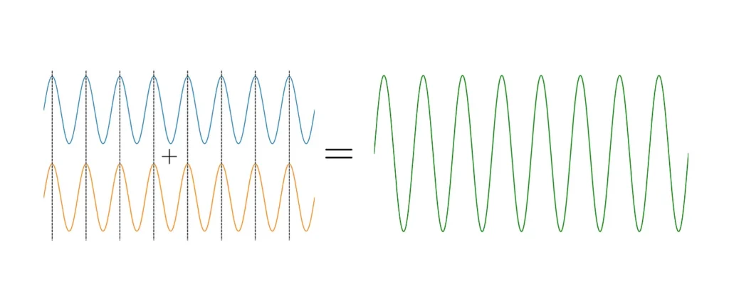
Two in-phase waves with the same frequency and amplitude, when added together, will constructively interfere to produce one wave of the same phase and frequency with greater amplitude
Light of a specific frequency performs a fixed number of oscillations over a given distance. If the paths are not the same length, then when the beams are recombined the relative phase will be different and the recombined beam will show the effects of interference.
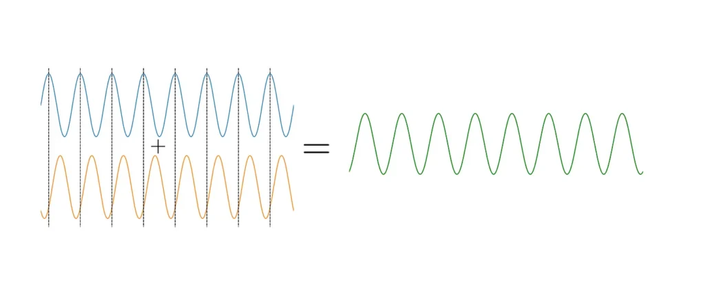
Two waves with the same amplitude and frequency but different phases destructively interfere to produce a new wave with a smaller amplitude and a different phase to both. By controlling the phase and amplitude of each wave, we can create a new wave with different properties. This is the fundamental principle by which we can encode information into a beam of light.
Because light has such a short wavelength, even tiny changes in distance along each path will produce detectable changes in phase. Interferometers come in many different forms; some are huge (the LIGO gravitational wave detectors are 4km long along each path or “arm” of the detector), and some are tiny. In our system, we cut micro-scale components called Mach-Zehnder interferometers (MZIs) into the silicon.
The Mach-Zehnder Interferometer
The phase-altering property of interferometers isn’t just useful for detecting changes in distance; they can also be used as a means of controlling the properties of light. We use MZIs to control the phase and amplitude of light passing through our silicon photonic circuit.
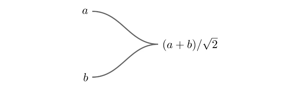
A silicon photonic MZI has a very simple structure. It starts when a single waveguide is split into two paths, each representing one of the arms of an interferometer. When we split the waveguide in two, light is distributed equally along each arm.
The amplitude of the optical field in each arm is equal to the input field divided by the square root of 2. This factor ensures that the total energy, proportional to the squared amplitude of the field, is conserved. This is illustrated in the diagram below. If we say that the original field has an amplitude equal to 1, the field in each branch has an amplitude 1/√2:

When two branches merge, the amplitude of the field is the sum of the amplitudes in each branch divided by √2 (again, this factor is required for energy conservation):
If the phase of light travelling along one arm changes relative to that of the light travelling down the other arm, recombining the two fields will create a field with different phase and amplitude to the input.
The paths themselves are cut into the silicon and can’t change in length, so we have to use a different method of altering the relative phases. Instead of changing the distance, we can achieve the same effect by changing the local speed of light along each arm by altering the refractive index of the silicon.
The phase of an optical field travelling througah a material is given by
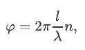
Where φ is the phase of the optical field, λ is the wavelength, l is the length of the path through the material, and n is the refractive index. Change n, and we introduce a proportional change in the phase.
There are a number of ways in which we can change n, and the method we choose can have a dramatic impact on the performance of the system. We’ll cover this subject in another article, but for now one of the simpler ways is by changing the temperature of the silicon waveguide.
This gives us a means of tuning the phase. From a mathematical point of view, if we say that the light entering one arm of an MZI has an amplitude equal to 1, changing the phase is equivalent to multiplying the input amplitude by a complex number with modulus 1. If you’re familiar with complex numbers, this can be written as multiplication with the exponential exp(i φ), which is usually written as e with the argument in superscript.
We can represent this schematically as:

with the input on the left and output on the right.
We can make a Mach Zehnder interferometer that uses only a single heater on one arm of the MZI, but it would not be able to change the modulus and phase independently. Instead, by using two heaters (one on each arm in what is known as a push-pull configuration), we only need to use half of the maximum temperature to cover the same phase range.
A single Mach-Zehnder interferometer performs the following tasks:
- A single input beam of light is separated into two by splitting the waveguide. The amplitude of the beam in each arm is given by the amplitude of the input beam divided by √2.
- The field in the upper branch is multiplied by the exponential of an imaginary number, adding φ₁ to its phase.
- The field in the lower branch is multiplied by the exponential of another imaginary number, adding φ₂ to its phase.
- At the recombination point, the fields are summed with their amplitudes divided by √2.
The amplitude of the recombined field is therefore:

Let x be a complex number that we want to encode into a beam of light. If its modulus is no larger than 1, we can encode x into the beam by choosing the phases such that

with the associated complex argument

The notation ‘mod’ indicates that the maximum range of the complex argument arg(x) can only lie between 0 and 2π. This is because a complex number is not changed by adding 2π to its phase, which amounts to a rotation by 360° in the complex plane.
The above gives us a method of linking numerical values with adjustments to the properties of light, allowing us to make the conversion from a digital representation of a number into an optical one. By using two arrays of multiple Mach Zehnder interferometers in series, we can perform these operations on many beams of light at once.
Optical Multiplication
However, we aren’t done quite yet. In our first article, we described how the Fourier transform can be used to simplify certain problems. Another very useful mathematical tool, the “convolution” of two functions, can be performed efficiently in Fourier space through the equation

The convolution equation; I and K are 2-dimensional arrays of data and the curved F represents the Fourier transform. Raising F to the negative power indicates the inverse Fourier transform.
If we already know the Fourier transforms of I and K (which we can rapidly calculate using our device) then we can perform the element-wise multiplication in this equation optically by using two arrays of MZIs in series, like so:
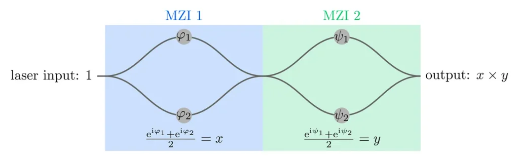
Here the numbers φ₁, φ₂, ψ₁, and ψ₂ are phase values which can be chosen at will by adjusting n. Passing the output of this multiplication into the free space optics will perform the inverse Fourier transform on the data, completing the calculation of the convolution of I and K.
If we don’t want to perform a multiplication (if, for instance, we are calculating the initial Fourier transform) then we are not obliged to do so; we can simply set the second MZI such that it does not alter the phase.
The convolution operation is a major part of executing a Convolutional Neural Network, or CNN. CNNs are well known as cutting-edge techniques in machine vision, but they have also been applied to a wider range of problems including network security analysis, the protein folding problem, and the task of predicting electron density parameters in complex quantum systems.
Not only is the optical Fourier transform naturally much faster than the electronic variant (both in terms of the number of operations and the maximum operating speed of an optical system), but the ability to simultaneously perform both the multiplication and inverse Fourier transformation required for the convolution in a single optical pass makes Fourier-optical computing a natural fit for high speed processing in machine vision tasks.
Putting it all together
Silicon photonics gives us everything we need to be able to reliably control light, but there’s still more work to do. So far, we have focused on how we can write digital information into light, but how do we get light into the system in the first place, and what do we do with it once we’ve finished altering it?
We want to be able to process as much data as possible in a single operation so we need multiple beams, as many as is practical. To get light into our chip, we start with a single source of laser light. This can be from an integrated laser built into the surrounding control electronics, or (as in the case of our prototype system) it can be generated by a desktop laser source.
We use a fibre-optic cable to convey light from the laser source to an input waveguide on the silicon photonic chip. We can then divide this single source of light in two by splitting this input waveguide into two paths, just as we do when making an MZI.
However, rather than recombining the two beams, we can split each beam again using the same method until we have as many individual beams as we like. This is called a branching-tree multiplexer. Of course, every time we split the waveguides we decrease the total optical power present in each beam, so there is a limit to how many beams we can make from a single laser source.

Once we have these beams, we then feed each waveguide into its own pair of MZIs where we perform the encoding and multiplication operations described above.
After encoding the light, we then want to create a 2-dimensional optical field that can be processed by a lens. In our system, each output waveguide carrying light processed by the MZI arrays feeds into a 2-dimensional grid of light-emitting grating couplers that lie just under the surface of the silicon photonic chip. These are structures cut into the waveguides which cause the light to reflect upwards.
This is where light leaves the silicon photonic system, with each individual beam carrying a different optical representation of a complex number. We’ll cover what happens to these beams of light in the next article.